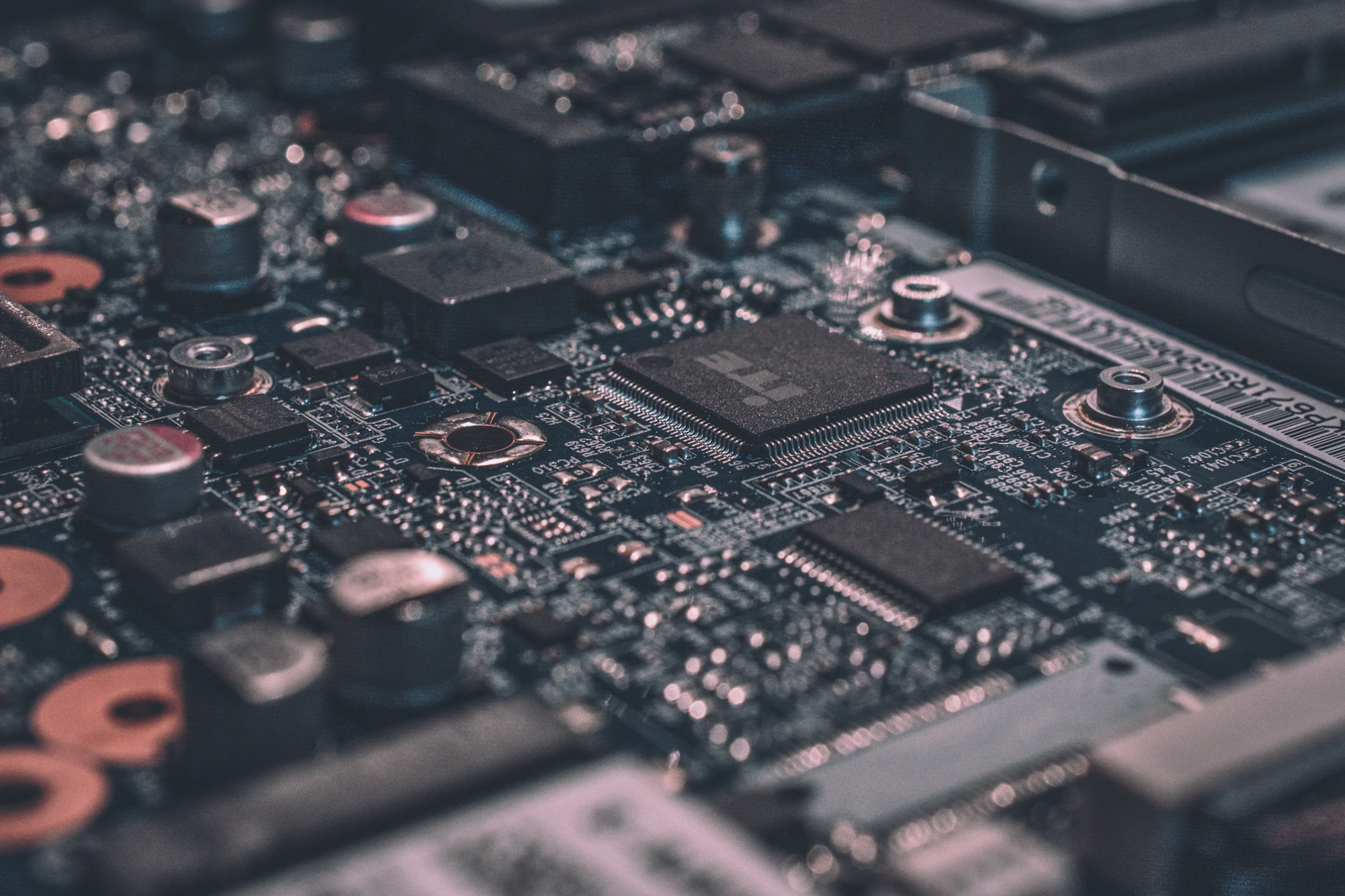
18.2 MΩ·cm Ultrapure Water System for Semiconductor Cleanroom
SECTOR 05 · ULTRAPURE GRADE

Engineered Water Architectures for
Semiconductor & Microelectronics.

Trace impurities destroy wafer yields. We deliver heavy-duty Double-Pass RO and EDI architectures designed to guarantee continuous 18.2 MΩ·cm ultrapure water (UPW) and recycle complex fab wastewater.

18.2 MΩ·cm UPW
EDI Integration
High-Yield Focus
Request UPW Layout

System Technical Specifications

Engineering Data Sheet
Capacity Range
10 - 1,000 m³/h
Scalable multi-train architecture.
Max Purity (UPW)
18.2 MΩ·cm
TOC < 1 ppb, Silica < 0.5 ppb.
Particles (>0.05μm)
< 1 count/mL
Absolute yield protection.
Deployment Format
Vertical Skid
High-density cleanroom footprint.

One Fab. Three Critical Streams.

We architect the complete, closed-loop water cycle to protect your wafer yields and environmental compliance.

STREAM 01 / PROCESS FEED

Ultrapure Water (UPW) Generation

Generating massive volumes of absolute 18.2 MΩ·cm water required for precise wafer washing and photolithography.

Solution: Double-Pass RO + EDI Skids
STREAM 02 / EFFLUENT

Fluoride & Heavy Metal Wastewater

Neutralizing highly toxic CMP slurry, hydrofluoric acid, and heavy metals to meet strict fab discharge thresholds.

Solution: Specialized Chemical Dosing + UF
STREAM 03 / RECOVERY

UPW Rinse Water Recycling

Pushing spent rinse water through specialized membranes to recover up to 85% back to the UPW makeup system.

Solution: Low-Fouling RO + Polishers
// SECTION 03 — ENGINEERING DIAGNOSTICS & CURES

Neutralizing the constraints of semiconductor fabrication.

Standard water filters are useless in a cleanroom. Microelectronics require absolute purity and zero-downtime architectures. Here is the deep-dive into how WANDONG ENVIRO architects around the three deadliest fab constraints.

01

The Yield Killer (Trace Impurities)

Even parts-per-trillion (ppt) of boron, silica, or organic carbon can short-circuit a microchip, destroying millions of dollars in wafer yields. Standard single-pass RO systems simply cannot achieve the ionic rejection required for modern sub-nanometer nodes.

The Engineered Cure: We implement Double-Pass RO + EDI Architectures. By utilizing genuine DuPont/Dow resins and continuous electrodeionization (EDI), we strip out 99.99% of dissolved ions. We guarantee absolute 18.2 MΩ·cm resistivity with zero particle shedding, protecting your production line at the molecular level.

Purity Matrix
Standard Single-Pass RO
Inconsistent Purity
Leaves trace ions; causes yield defects.
Wandong DP-RO + EDI
18.2 MΩ·cm
✓ ABSOLUTE YIELD PROTECTION

02

The Water Consumption Bottleneck

A modern semiconductor fab consumes millions of gallons of ultrapure water daily. Relying solely on municipal intake not only incurs massive operational costs but also exposes the entire facility to catastrophic production halts during regional droughts or water restrictions.

The Engineered Cure: We engineer Rinse Water Recovery Loops. By intercepting low-TDS spent rinse water from the cleanroom, we process it through dedicated UF/RO skids, returning up to 85% back to the UPW makeup system. This slashes municipal reliance and builds resilience against water scarcity.

Supply Resilience Matrix
Single-Pass Fab
High Vulnerability
100% dependent on municipal grid.
WANDONG Closed-Loop
85% Independence
Recycles spent rinse water continuously.
Strategic Advantage
Drought Immunity
Guarantees uptime during water shortages.

03

Cleanroom Footprint Constraints

Fab floor space is the most expensive real estate on earth. Traditional, sprawling water treatment plants waste valuable square footage that should be dedicated to revenue-generating production tools and lithography machines.

The Engineered Cure: We deliver High-Density Skid-Mounted UPW Systems. Our multi-tier stainless steel skids stack RO and EDI modules vertically, shrinking the mechanical footprint by up to 40%. The entire architecture is pre-piped and pre-wired, allowing for rapid drop-in installation through standard facility doors with zero civil work.

Footprint Matrix
Traditional UPW Plant
Sprawling
Eats up valuable cleanroom sub-fab space.
WANDONG Vertical Skids
- 40% Space
High-density 3D piping architecture.
Installation Method
Drop-in Ready
Fits through standard facility doors.
// SECTION 03.5 — THE TCO ECONOMICS

Stop Bleeding Fab Margins.

Compare the cost of single-pass municipal consumption vs. investing in a WANDONG UPW Recovery architecture.

"Single-Pass" Model

Equipment CAPEXLow
Municipal Intake Bills (5 Yrs)Massive
Water Supply RiskHigh
5-YEAR FINANCIAL VERDICT
HIGH VULNERABILITY
The WANDONG Advantage

UPW Recovery Plant

Equipment CAPEX (UF + RO)Investment
Freshwater Bills (85% Reduction)Minimal
Water Supply RiskEliminated
Net Capital Retained+ Millions
PROFIT
5-YEAR FINANCIAL VERDICT
ROI < 18 MONTHS
/ SECTION 04 — ENGINEERING BLUEPRINT

The UPW Generation Cycle.

We utilize a heavy-duty, multi-barrier process block flow that guarantees stable generation of 18.2 MΩ·cm ultrapure water for sub-nanometer wafer fabrication.

TOPOLOGY: UF + DP-RO + EDI
RECOVERY: 80% - 90%
APPLICATION: SEMICONDUCTOR UPW
CONTROL: SIEMENS S7 PLC
STEP-01
Ultrafiltration (UF)
0.02μm PVDF
Absolute barrier for particles and colloids. Drops SDI < 1.
STEP-02
1st Pass RO
High Rejection Elements
Removes 99% of bulk dissolved ions, silica, and organics.
NaOH Dosing (CO2 Removal)
STEP-03
2nd Pass RO Stack
DOW LE Elements
Polishes permeate to < 5 µS/cm.
CORE
STEP-04 ♦

EDI Stack

Electrodeionization

Continuous electrical regeneration. Produces 18.2 MΩ·cm ultrapure water.

STEP-05 ★

UPW Storage

Nitrogen Blanketed

Prevents CO2 ingress and airborne contamination before final polish.

STEP-06 ⚠

Final Polish

185nm UV + 0.05μm Filter
Destroys trace TOC and captures resin fines before wafer contact.
INLET (CITY / REUSE)
TDS < 500 mg/L
OUTLET RESISTIVITY
18.2 MΩ·cm
TOC LEVEL
< 1 ppb
PARTICLES (>0.05μm)
< 1 count/mL
/ SECTION-05A / LIMITS

Inlet Boundary
Conditions.

City water or fab reuse feed must meet the following parameters before entering the UPW generation skid to prevent irreversible membrane and resin damage.

PARAMETER MAX LIMIT (RO FEED)
TDS (Total Dissolved Solids)< 500 mg/L
SDI₁₅< 3.0
TOC (Total Organic Carbon)< 2.0 ppm
Free ChlorineStrictly Not Detected
/ SECTION-05B / COMMITMENT

Target UPW
Performance Guarantee.

When inlet conditions are met, WANDONG ENVIRO contractually guarantees the following absolute purity standards for semiconductor fabrication.

OUTPUT METRIC GUARANTEED VALUE
Resistivity (@ 25°C)18.2 MΩ·cm
TOC (Total Organic Carbon)< 1.0 ppb
Dissolved Silica< 0.5 ppb
Particles (> 0.05μm)< 1 count/mL
// SECTION 06 — AUTOMATION PROTOCOLS

Zero-Downtime Automation.
Protecting the Yield.

Semiconductor fabs run 24/7/365. Unplanned UPW downtime means catastrophic yield loss. Our Siemens PLCs are programmed with redundant fail-safes and dynamic monitoring to ensure continuous 18.2 MΩ·cm delivery.

Even a momentary dip in resistivity can ruin a batch of wafers. We design our control systems not just to operate, but to autonomously anticipate and mitigate risks before they reach the cleanroom.

We hardcode N+1 Redundancy Logic into the system. If a primary high-pressure pump or EDI module experiences a fault, the PLC instantly switches to the hot-standby unit in milliseconds, ensuring zero interruption to your UPW flow.

Automated Quality Divert

Inline precision sensors constantly monitor resistivity and TOC. If resistivity drops below 18.0 MΩ·cm, the system triggers an immediate alarm and automatically diverts the off-spec water to the drain or recovery loop, physically preventing it from ever reaching the wafer washing stations.

Fab Control Logic
01. Dual-Redundant PLC HOT STANDBY
02. Continuous EDI Tuning AUTO-VOLTAGE
03. Resistivity Drop Alarm < 18.0 MΩ·cm WARNING
04. TOC Spike Divert AUTO-REJECT
> UPW_STATUS: CRITICAL_OPS_NORMAL
> RESISTIVITY: 18.24 MΩ·cm [STABLE]
> TOC_LEVEL: 0.8 ppb [PASS]
> REDUNDANT_PUMP_B: STANDBY_READY.
// SECTION 07 — GLOBAL SUPPLY CHAIN

Tier-1 Components. Zero Compromise.

DuPont™®
GRUNDFOS
SIEMENS
Danfoss
Schneider
// SECTION 08 — INDUSTRIAL LOGISTICS

Shipping & Footprint Matrix.

High-density vertical skids designed to drop directly into existing cleanroom sub-fabs, maximizing your production floor space.

System Model Capacity (m³/day) Application Format
WD-UPW-100 100 m³/day Lab / Micro-Fab UPW Sanitary Skid
WD-UPW-500 500 m³/day Mid-tier Semiconductor UPW Multi-tier Skid
WD-REUSE-1000 1,000 m³/day Wafer Rinse Recovery Open-Frame Skid
WD-CMP-250 250 m³/day CMP Slurry Treatment Custom Modular
// SECTION 09 — EHS COMPLIANCE

Fab-Grade Reliability.

In the semiconductor industry, compliance isn't just about the environment—it's about protecting the product. Our architectures ensure you stay ahead of both yield requirements and environmental regulations.

SEMI Standards Alignment

Our UPW architectures strictly comply with SEMI F63 guidelines for ultrapure water used in semiconductor manufacturing.

ISO 9001 / 14001

Manufactured under strict quality control to ensure zero particle shedding and full environmental compliance.

Yield Protection Guarantee

If the feed water matches the provided report, we contractually guarantee the 18.2 MΩ·cm resistivity and TOC limits. No excuses.

// SECTION 10 — TECHNICAL Q&A

Hardcore FAQ.
Engineering-Grade Answers.

Q-01 / EDI VS MIXED BED

Why use EDI instead of traditional Mixed Bed DI?

+
EDI (Electrodeionization) uses electricity to continuously regenerate the resin, eliminating the need for hazardous acid and caustic chemicals on the fab floor. It provides more stable 18.2 MΩ·cm water, eliminates the downtime associated with resin regeneration, and drastically reduces OPEX and safety risks.
Q-02 / TOC REMOVAL

How do you achieve sub-ppb TOC levels?

+
We deploy a multi-barrier approach utilizing 185nm UV oxidation lamps to break down organic bonds, followed by specialized polishing resins and ultrafiltration to capture the ionized fragments. This architecture guarantees TOC < 1 ppb, preventing organic hazing on the wafers.
Q-03 / REDUNDANCY

What happens if a primary pump fails?

+
Our fab-grade skids are designed with N+1 or 2N redundancy for all critical rotating equipment (Grundfos pumps) and sensors. The Siemens PLC automatically switches to the standby unit in milliseconds, ensuring zero interruption to your production line.
Q-04 / BORON & SILICA

How do you guarantee Boron and Silica removal for sub-nanometer nodes?

+
Boron and Silica are weakly ionized and difficult to remove. We utilize a Double-Pass RO architecture with precise inter-stage pH adjustment (NaOH dosing) to fully ionize these contaminants, allowing the second-pass RO and final EDI stack to reject them to < 0.5 ppb levels.
Q-05 / CLEANROOM FOOTPRINT

Our sub-fab space is extremely limited. Can the system fit?

+
Yes. We utilize 3D high-density piping design to stack the RO vessels and EDI modules vertically. This "Vertical Skid" approach reduces the mechanical footprint by up to 40% compared to traditional flat-layout plants, easily fitting through standard facility double-doors.
Q-06 / FAT & VALIDATION

Do you provide full validation documentation (IQ/OQ/PQ)?

+
Absolutely. We provide comprehensive documentation packages to support your facility's validation process, including Installation Qualification (IQ) and Operational Qualification (OQ) protocols. We also conduct a full wet FAT (Factory Acceptance Test) before shipping to prove the 18.2 MΩ·cm output.
// SECTION 11 — VERIFIED DEPLOYMENTS

Proof in the field.

View All Case Studies →
// SECTION 12 — INITIATE PROTOCOL

SECURE YOUR FAB'S
UPW SUPPLY.

You focus on pushing Moore's Law and maximizing yields; let us handle the absolute water purity. Submit your feed parameters, and our engineering team will architect a custom UPW solution guaranteed to perform.

1h
INITIAL RESPONSE
1-ON-1
CUSTOM PROPOSAL
$0
CONSULTATION FEE
// SECURE YOUR SUPPLY CHAIN

Request Firm Quote & P&ID

Receive a custom P&ID and Factory-Direct project budget within 48 hours.

DROP FILE OR CLICK
.PDF / .XLSX / .CSV / MAX 10MB
AVG. RESPONSE: < 4 HRS · NDA AVAILABLE ON REQUEST
18.2 MΩ·cm Purity Zero Yield Loss Fast ROI